“Development of a Low Temperature High Quality Silicon Oxide Deposition Process”
Carlos
Eduardo Viana - ceviana@lsi.usp.br
High
quality silicon oxide thin films deposited at low temperature have many applications
in microelectronics such as: passivation coatings, interlevel dielectric,
and gate dielectric in metal oxide semiconductor field effect transistors
(MOSFET's) and thin films transistors (TFTs)[1].
Plasma Enhanced Chemical Vapor Deposition (PECVD) is one of the most promising
processes used in these technologies due to its suitable characteristics such
as good step coverage, low deposition temperature, high deposition rate, etc.[2].
The
silicon oxide deposition process was carried out in the following basic conditions:
process pressure (P) of 1 Torr; temperature (T) of 375°C; oxygen flow (FO2) of 450
sccm and RF power (Wrf) of 400 W.
The thermal silicon oxide refractive index was used
as a criteria to choose the best deposited silicon oxides. Using 7.5 sccm
of TEOS flow, 50 sccm of argon and 10 mm of distance between electrodes,
it was observed that the refractive index is very close to the refractive
index of thermal silicon oxide (refractive index ≈ 1.464).
Table 1: Electrical properties of deposited silicon oxide, extracted from HF-CV plots.
|
Sample
|
Vfb:
|
eox:
|
Qss:
|
|
L1
|
-4.31
|
9.3
|
1.71
x1012
|
|
L1 A
|
-3.73
|
8.9
|
1.42
x1012
|
On Table 1, the effective charge density is high mainly because in the PECVD process, using TEOS as silicon source, there is an incorporation of carbon into the deposited silicon oxide[5].
The TRXFA measurements showed that the deposition process introduces a metallic contamination in the silicon/SiO2 interface (Fe » 4.574 x 1012 cm-2, Zn » 1.997 x 1012 cm-2 and Cu » 2.409 x 1012 cm-2).
These metallic impurities are also responsible for the high effective charge density found in the capacitors.
|
|
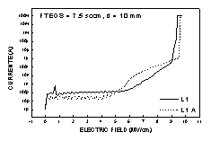
Figure 1: IE plots in the accumulation region of the samples: (L1) as deposited and (L1 A) after annealing.
The IE plot of the sample L1 shows the absence of any trapping ledge in the electron injection region (more than 5 MV/cm), which indicates a low concentration of bulk traps[6]. For the annealed sample, trapping ledges are observed indicating a high concentration of bulk traps. This effect can be explained by the structural rearrangement occurred during the high temperature step.
Table 2: Leakage current and breakdown strength calculated from the IE plots.
|
Sample
|
ILK (A):
|
Ebd:
|
|
L1
|
1.06
x 10-10
|
9.01
|
|
L1 A
|
2.35
x 10-11
|
9.43
|
The annealed samples on Table 2 showed a higher breakdown strength and a lower leakage current. Probably, the rearrangement of the atomic structure in the annealed samples eliminates -OH groups and H2O incorporated during the deposition process improving the electrical characteristics of the deposited films.
The metallic contamination during the deposition process increased the effective charge density. A deposition process optimization is necessary to minimize the effect of the metallic contamination. After this optimization process, the deposited silicon oxide quality will be suitable for use as gate dielectric in MOS technology.