Annealing Effects
in the PECVD-SiO2 Deposited Using TEOS, Ar and O2 Mixture
Carlos Eduardo Viana
ceviana@lsi.usp.br
Ph.D. Research
( Advisor: Prof. Dr. Nilton Itiro Morimoto)
High quality silicon oxide thin films, deposited in low temperature, have many applications in microelectronics such as: passivation coatings, interlevel dielectric, and gate dielectric involved as well in integrated metal oxide semiconductor field effect transistors (MOSFETs) as in thin films transistors (TFTs)[1],[2],[3]. Plasma Enhanced Chemical Vapor Deposition (PECVD) is one of the most important process used in these technologies due to its suitable characteristics such as good step coverage, low deposition temperature, high deposition rate, etc.[2].
The home made PECVD cluster tool system, used in this study, was described elsewhere[4],[5]. It has three process chambers, a load lock and a sample manipulation chamber.
The silicon oxide deposition process is carried out in the basic process conditions: the TEOS, oxygen and argon flows are 7.5, 450, and 0 to 200 sccm respectively, process pressure is 1 Torr, temperature is 375°C, RF power is 400 W and distance between electrodes is 10 mm.
|
|
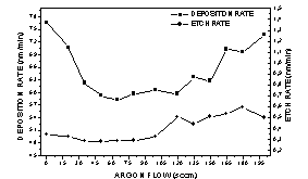
Figure 1: Deposition and etch rates of the silicon oxide films as a function of the argon flow.
The FTIRS spectra showed a small absorbance band in 1234 cm-1 that is attributed to the Si‑OCH3 bonds.
Figure 2 shows the typical I-E curves obtained from the MOS capacitors implemented with silicon oxides deposited with 150 sccm of argon flow. The I-E curves are parametrized with the annealing time.
|
|
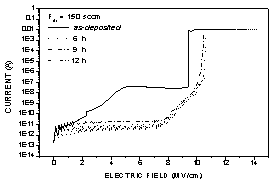
Figure 2: I-E curve from MOS capacitor implemented with an argon flow of 150 sccm.
Table 1 shows the parameters extracted from the I-E and C-V curves. The leakage current (ILK) values were obtained with a 4 MV/cm electrical field applied to the capacitors.
Table 1: Leakage current and breakdown strength extracted from the I-E curves.
|
Ar flow (sccm) |
Annealing time
(h) |
ILK
(pA) at 4 MV/cm |
EBD
(MV/cm-1) |
Qss (1012 cm-2) |
|
|
as‑dep. |
4270 |
9.38 |
0.73 |
|
150 |
6 |
5.3 |
10.5 |
1.46 |
|
|
9 |
19 |
10.2 |
1.71 |
|
|
12 |
4 |
10.5 |
2.05 |
We can observe an improvement of the leakage current as well as in breakdown strength in the annealed samples. The annealing time has low influence on the electrical parameters. The I-E curve of the as-deposited sample shows a high leakage current that is related with the trapped charges in the silicon oxide film[6]. After the annealing process, at low temperature, these trapped charges are removed or rearranged inside the oxide. However, the atomic structure of the silicon oxide is not significantly changed, because the annealing temperature is rather low (600°C). Then, atomic vacancies can be generated due to the trapped charge rearrangement increasing the effective charge density (Qss).
The influence of argon in the deposition process of the PECVD silicon oxide was analyzed. An annealing process at low temperature promotes a rearrangement of the trapped charges into the silicon oxide layer. We observed an improvement in the breakdown strength, but the effective charge density increased. The annealing time has low influence in the electrical characteristics of the deposited film.